Computer Architecture Fundamentals
Begin
13 pages · ~26 min
Computer Architecture Fundamentals
A foundational course for beginners exploring the core components of a computer system, including CPU, memory, and I/O.
What you’ll learn
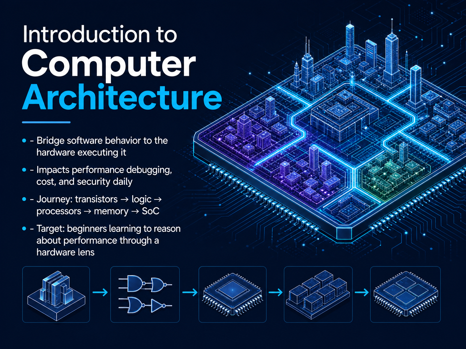
- 01Introduction to Computer ArchitectureWelcome. This course is about understanding the hidden logic inside every computer--the hardware that actually runs your code. Our goal is to bridge the gap between software behavior and the physical machine. When you finish, you will see how everyday decisions in code directly impact performance, cost, and even security. We start at the lowest level, with transistors, and build upward. We will see how transistors form logic gates, how gates become processors, how processors connect to memory, and finally how everything comes together in a modern System-on-a-Chip. This is a journey for curious beginners. You don't need a hardware background, just a desire to connect what you type to what the silicon does. By the end, you will have a new lens for reasoning about performance. Next, we will look at the big picture: from high-level code all the way down to electrical signals.martinkalema.github.iojincheng.ligithub.com+21 min
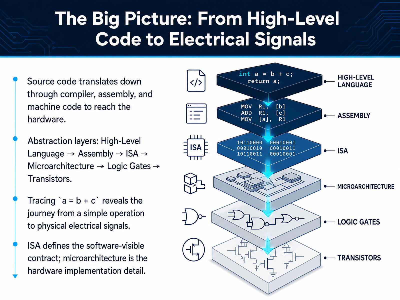
- 02The Big Picture: From High-Level Code to Electrical SignalsLet's trace what really happens when a program runs. You write a simple line of high-level code, like a equals b plus c. That one line triggers a chain of translations. First, a compiler turns your code into assembly language. Then an assembler converts that into machine code, the binary instructions your processor actually reads. We describe this path using abstraction layers. High-level language sits on top, then assembly, then the instruction set architecture, or ISA. Below that is the microarchitecture, which is the hardware organization that implements the ISA. Deeper still are logic gates and finally transistors where electrical signals do the work. Think of the ISA as the contract software sees. It defines the instructions, registers, and memory model. The microarchitecture is the hidden implementation detail. It decides how many cores, caches, and pipelines deliver that contract. Two chips can share the same ISA but have completely different microarchitectures, which is why the same binary runs on both but performance can differ. Coming up next, we look closer at that programmer's contract in 'The Programmer's Contract: Instruction Set Architecture (ISA).'
 cs.stackexchange.comgeeksforgeeks.orgcompilersutra.com+22 min
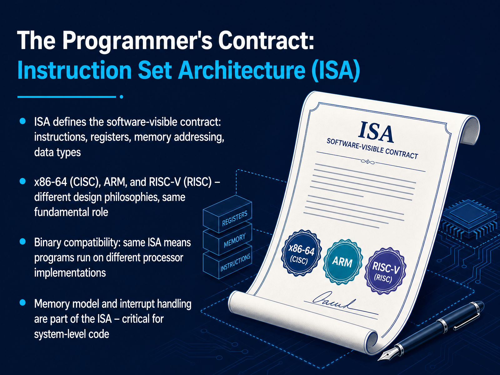
 - 03The Programmer's Contract: Instruction Set Architecture (ISA)Now let's look at the Programmer's Contract, the Instruction Set Architecture, or ISA. Think of the ISA as the formal boundary between the software you write and the hardware that runs it. It defines everything software can see and rely on: the available instructions, the registers, how memory is addressed, and the supported data types. Different ISAs reflect different design philosophies. For example, x86-64 is a CISC design, with many complex instructions. ARM and RISC-V are RISC designs, focused on a smaller set of simpler instructions. Despite those differences, they all serve the same fundamental role. A key superpower of the ISA is binary compatibility. If two processors implement the same ISA, like different Intel and AMD chips, the exact same program can run on both without modification. The memory model and interrupt handling are also part of this contract, which is critical for writing reliable system-level code. This contract is what makes the software ecosystem possible. Now, let's go inside the processor to see how this contract is actually fulfilled. That's the microarchitecture.
 cs.stackexchange.comgeeksforgeeks.orgcompilersutra.com+22 min
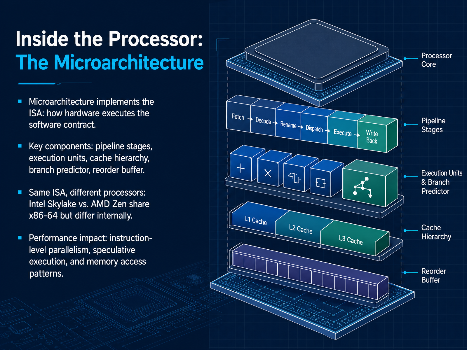
 - 04Inside the Processor: The MicroarchitectureNow we step inside the processor itself, to the microarchitecture. If the ISA is the software contract, the microarchitecture is the hardware that fulfills it. Think of it as the engine room. Key components here include pipeline stages, where instructions are broken into steps and overlapped like an assembly line. Execution units do the actual arithmetic and logic. The cache hierarchy holds data close for fast access. A branch predictor guesses which way a program will go, and a reorder buffer lets the processor execute instructions out of order while keeping the final results correct. This is why two processors can share the same ISA, like x86-64, but behave very differently. Intel Skylake and AMD Zen both understand the same instructions, yet their internal designs differ completely. The real performance impact comes from how these pieces work together. It is about instruction-level parallelism, speculatively executing work ahead of time, and how data flows through memory. Next, we will look at the fundamental building blocks that make all of this possible: transistors, logic gates, and sequential logic.
 cs.stackexchange.comgeeksforgeeks.orgcompilersutra.com+22 min
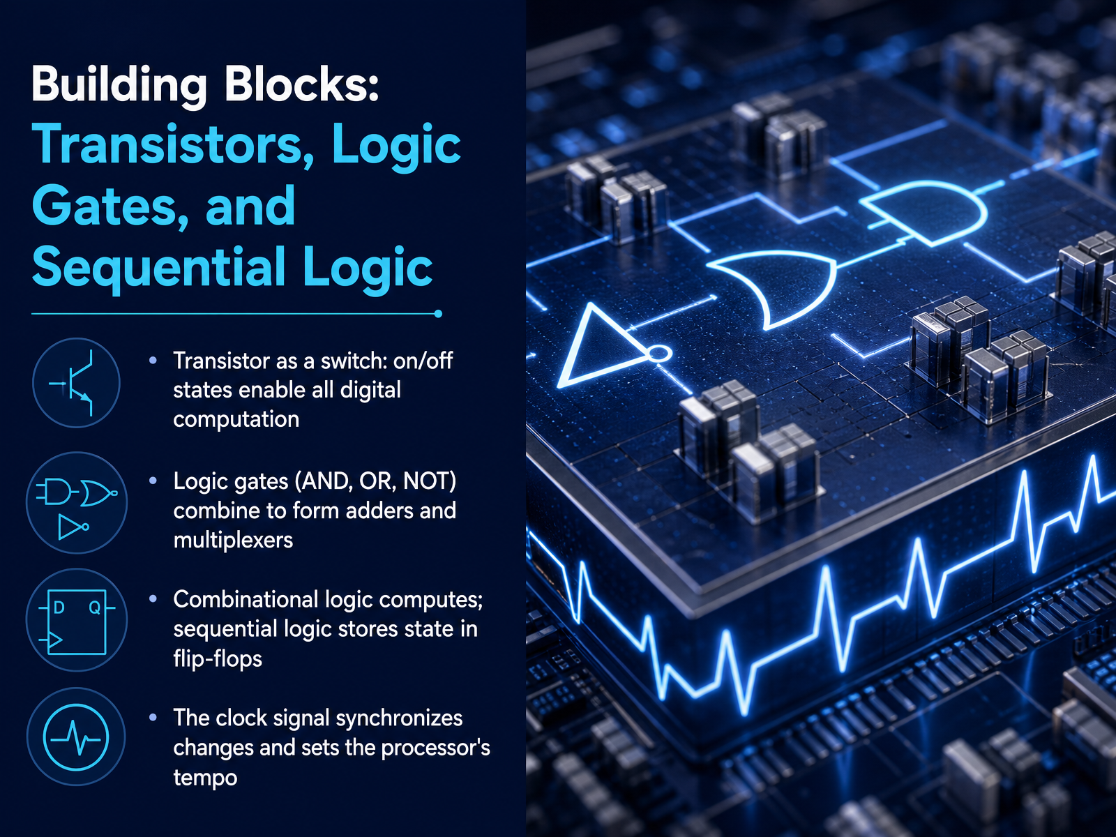
 - 05Building Blocks: Transistors, Logic Gates, and Sequential LogicNow let's look at the smallest building blocks. The fundamental switch inside every digital chip is the transistor. It only has two states: on or off. Those two states represent the ones and zeros of binary data. From these simple switches, we build logic gates. An AND gate outputs on only if all its inputs are on. An OR gate outputs on if at least one input is on. A NOT gate simply flips the state. We combine these gates to create larger structures like adders, which do arithmetic, and multiplexers, which route data. This is called combinational logic. It computes outputs based purely on current inputs. But a computer also needs memory. Sequential logic uses flip-flops to store a bit of information and hold that state. Finally, a central clock signal coordinates everything. It ticks at a steady rhythm, telling all these parts exactly when to sample their inputs and change their outputs. This sets the processor's tempo. Next, we will see how these pieces come together inside the Arithmetic Logic Unit, or ALU.
 2 min
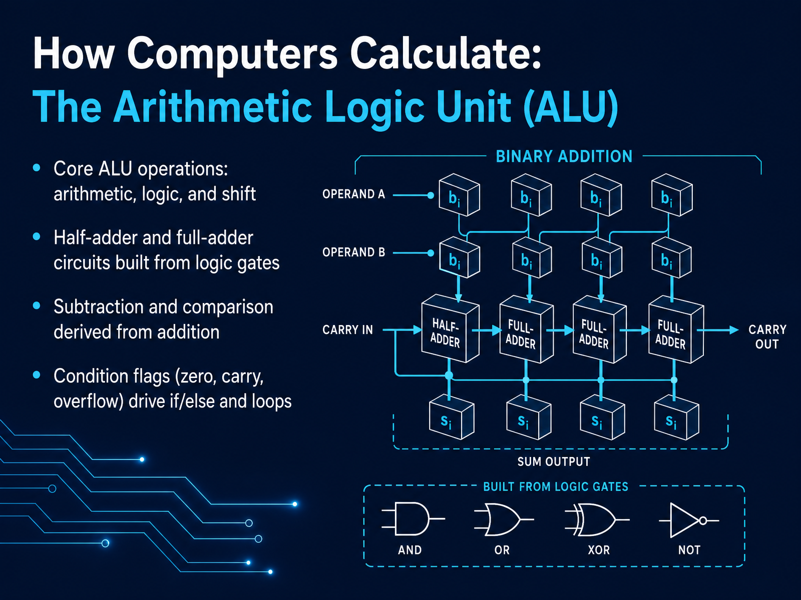
2 min - 06How Computers Calculate: The Arithmetic Logic Unit (ALU)Now let's look inside the chip at the part that does the actual math. It's called the Arithmetic Logic Unit, or ALU. The ALU performs three core types of operations. First, arithmetic, like addition and subtraction. Second, logic, such as AND, OR, and NOT. And third, shift operations that move bits left or right. At its heart, the ALU is built from tiny circuits called adders. A half-adder adds two bits and produces a sum and a carry. A full-adder also includes a carry-in from a previous stage. By chaining full-adders together, we can add larger binary numbers. Subtraction is clever. It's done by adding the two's complement of a number. Comparing two numbers is also done with subtraction. The ALU simply checks if the result is zero or negative. Every calculation sets special condition flags. A zero flag turns on when the result is zero. A carry flag signals an overflow from the highest bit. An overflow flag catches sign errors. These flags are what drive if-else statements and loops in your code. The branch decision literally depends on a single bit. Next, we'll see how the ALU fits into the bigger picture in The Processor Core: Datapath and Control.
 2 min
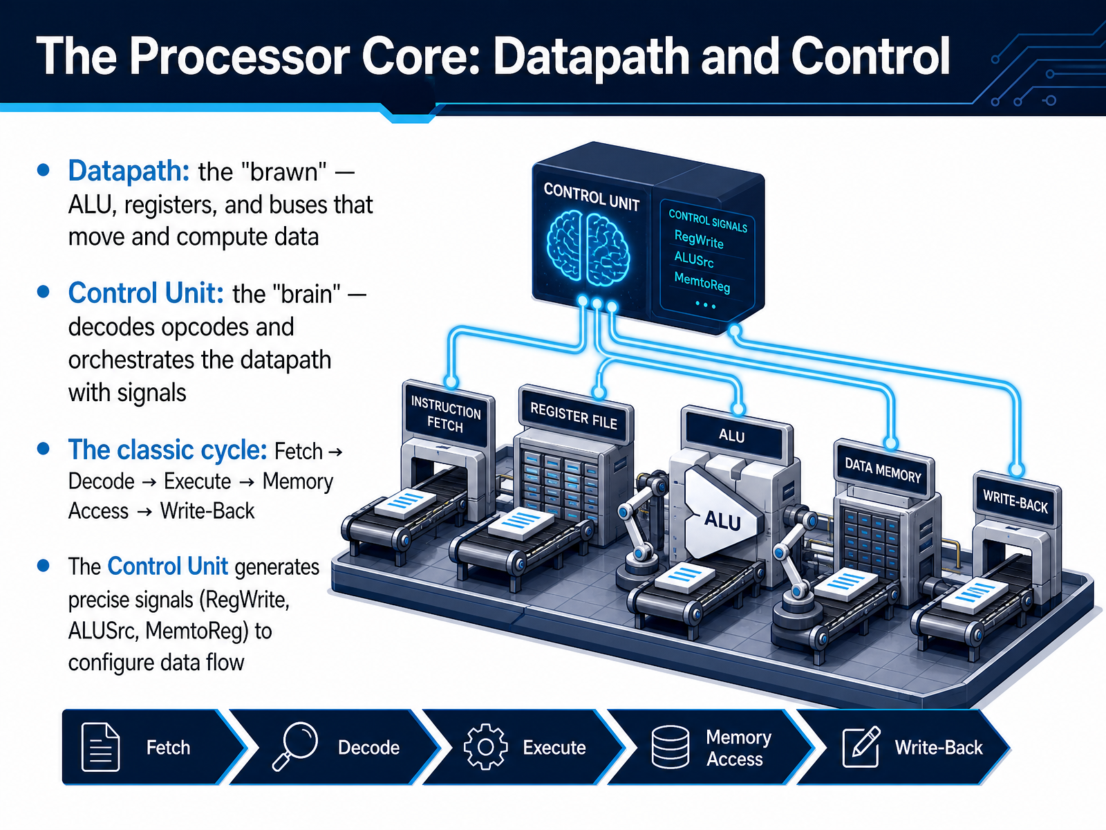
2 min - 07The Processor Core: Datapath and ControlNow let's zoom inside the processor core itself. The core has two main parts that work together, the datapath and the control. Think of the datapath as the brawn. It contains the hardware that actually moves and computes data, the ALU, the registers, and the internal buses. The control unit is the brain. It decodes the opcode from the instruction and orchestrates the datapath with precise signals. The classic cycle that drives everything is Fetch, Decode, Execute, Memory Access, and Write-Back. During each step, the control unit generates specific signals. For example, a signal called RegWrite tells the register file to store a result. Another signal, ALUSrc, selects whether the ALU gets its second input from a register or from an immediate value in the instruction. A signal called MemtoReg decides if the data written back to the register comes from the ALU or from data memory. These signals configure the datapath on the fly, so the same hardware can handle an add instruction, a load from memory, or a store to memory. Next, we will explore the memory hierarchy and why your laptop has cache, RAM, and SSD.
 notes.cs61c.orgcise.ufl.edupeople.duke.edu+22 min
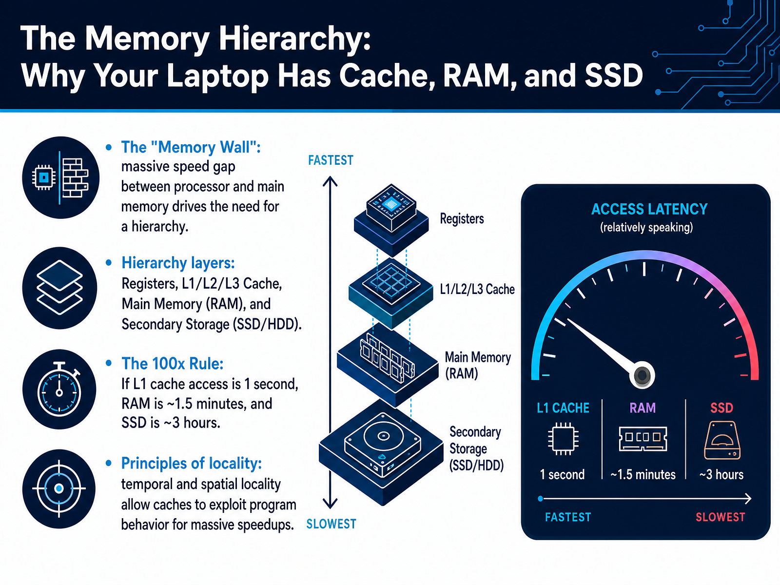
 - 08The Memory Hierarchy: Why Your Laptop Has Cache, RAM, and SSDHere is where the speed gap between the processor and main memory really shows itself. We call this the Memory Wall. The CPU can process an instruction in under a nanosecond, but fetching data from RAM takes roughly a hundred nanoseconds. To bridge this gap, we use a memory hierarchy. At the top, inside the CPU core, we have registers and tiny, fast L1, L2, and L3 caches. Below that sits main memory, your RAM. And at the bottom, we have larger, persistent storage like your SSD. To make this concrete, let's use the one-hundred-x rule. If accessing L1 cache felt like one second, grabbing data from RAM would feel like one and a half minutes. Reading from a fast SSD would be like waiting three hours. This works because of two principles of locality. Temporal locality means if you access a piece of data once, you will likely use it again soon. Spatial locality means if you access one memory location, you will probably access its neighbors next. Caches hold onto this hot data, keeping your CPU fed and delivering massive speedups. Next, we will look at cache mechanics and their impact on your code.
 martinkalema.github.iojincheng.ligithub.com+22 min
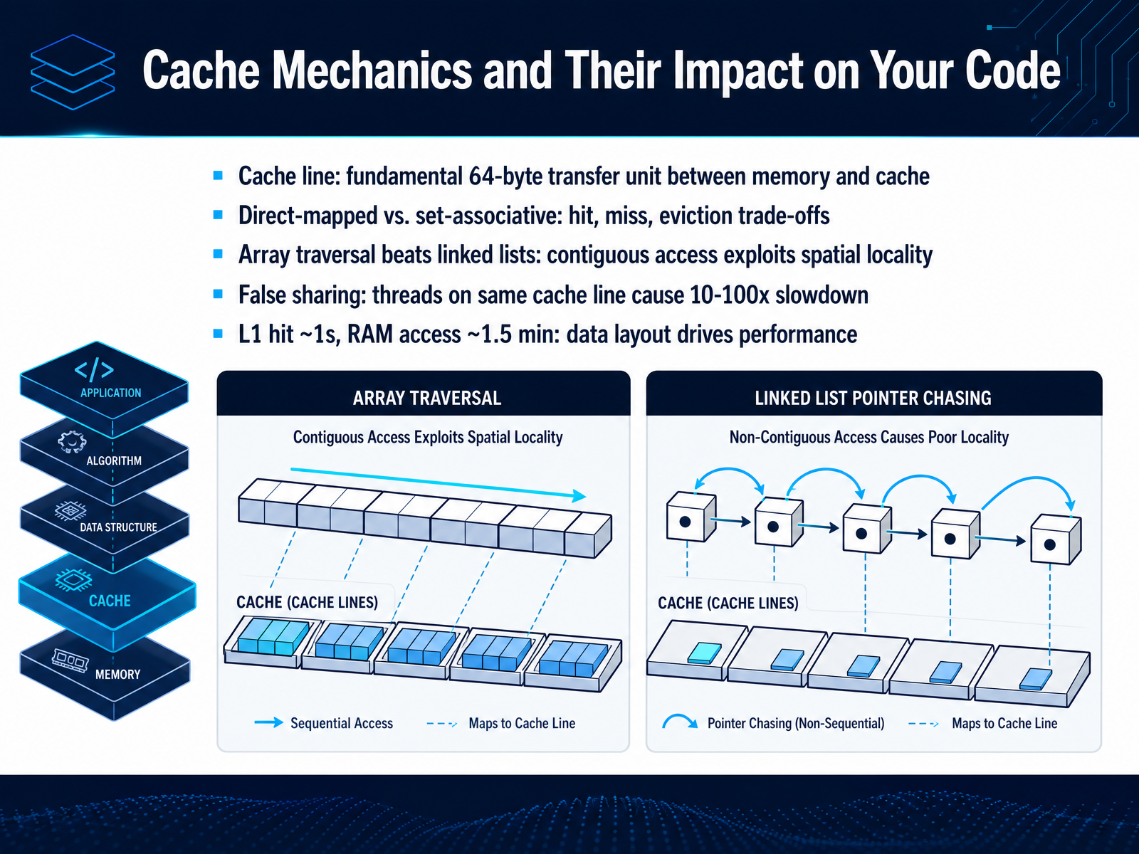
 - 09Cache Mechanics and Their Impact on Your CodeNow let's look at how the cache actually works, and why it changes the way you write code. The cache moves data in fixed-size chunks called cache lines. Each line is sixty-four bytes. When your program asks for one variable, the processor pulls in the entire sixty-four-byte block that surrounds it. Then we have different cache architectures. In a direct-mapped cache, each memory address can only live in one specific cache slot. If two addresses fight for the same slot, you get constant eviction and misses. Set-associative caches relax this by allowing an address to live in a few possible slots, which reduces conflict. But the real performance win comes from writing code that respects spatial locality. Looping through an array is fast because you access consecutive memory addresses inside the same cache line. Walking a linked list is slow because each node can be anywhere in memory, causing a miss on almost every step. In multi-threaded code, watch out for false sharing. When two threads write to different variables that happen to sit on the same cache line, the line bounces between cores. This can slow your code down by a factor of ten to one hundred. To put this in perspective, let's rescale time. If an L1 cache hit felt like one second, then fetching that same data from main memory would feel like a minute and a half. Data layout is not a micro-optimization. It is the foundation of performance. Next, we'll explore pipelining, which is the assembly line for instructions inside the CPU.
 martinkalema.github.iojincheng.ligithub.com+22 min
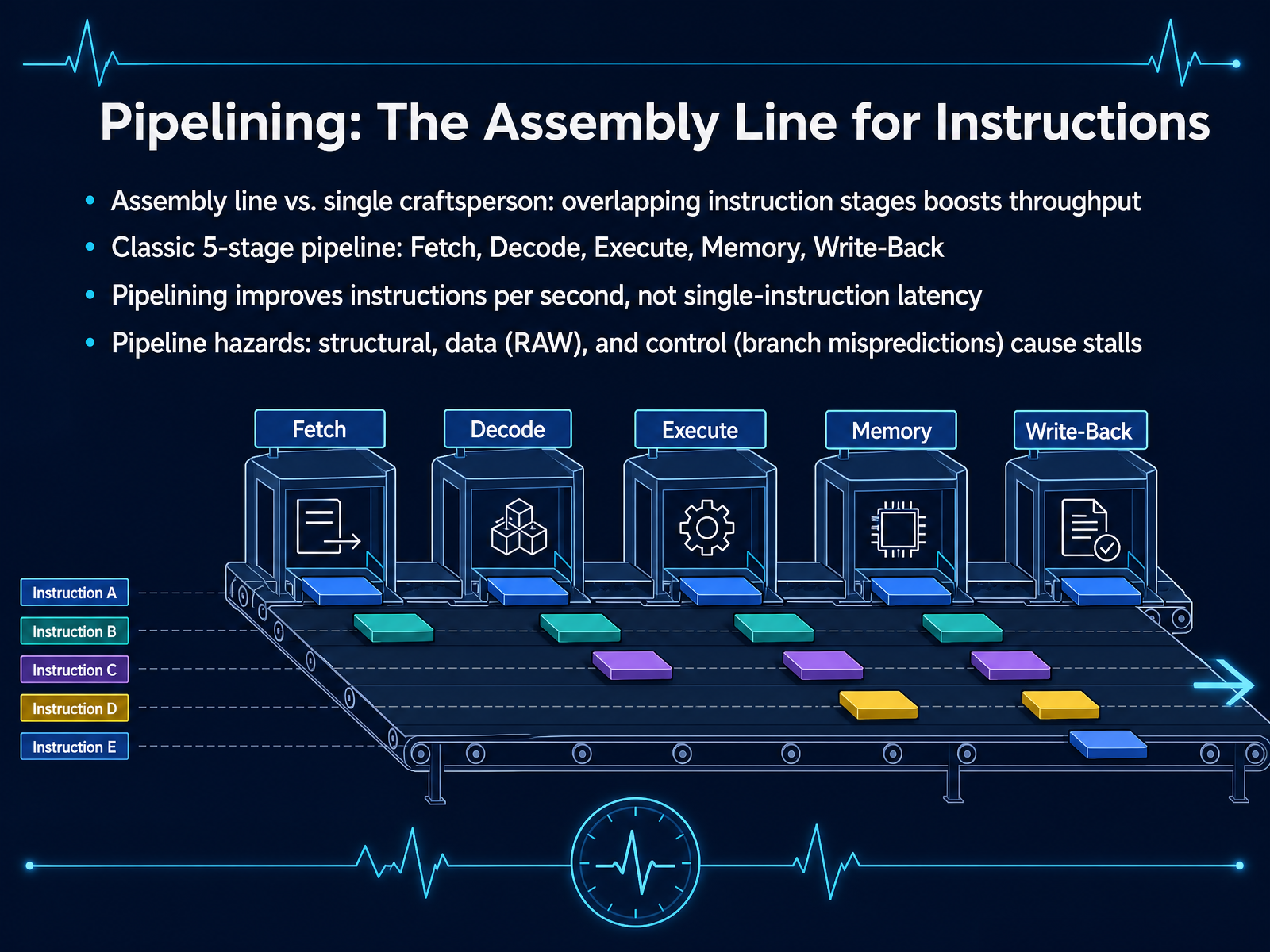
 - 10Pipelining: The Assembly Line for InstructionsNow, let's look at a technique that makes modern processors so fast: pipelining. Think of it like an assembly line. Instead of a single craftsperson building one complete product at a time, you have multiple stations, each doing a specific task. In a processor, we overlap the stages of instruction execution. The classic pipeline has five stages. First, Fetch: getting the instruction from memory. Second, Decode: figuring out what the instruction means. Third, Execute: performing the actual calculation. Fourth, Memory: if the instruction needs to read or write data. And fifth, Write-Back: storing the result. Here's a key point. Pipelining increases the number of instructions finished per second, what we call throughput. But it does not reduce the time it takes for any single instruction to complete. Sometimes, the pipeline can stall. These stalls are called hazards. A structural hazard is when two instructions need the same hardware resource. A data hazard, like a Read After Write, is when an instruction depends on the result of a previous one that isn't ready yet. And a control hazard happens when a branch instruction is mispredicted, and the processor has fetched the wrong instructions. Next, we'll explore how processors overcome these limits with advanced performance techniques, like out-of-order and speculative execution.
 2 min
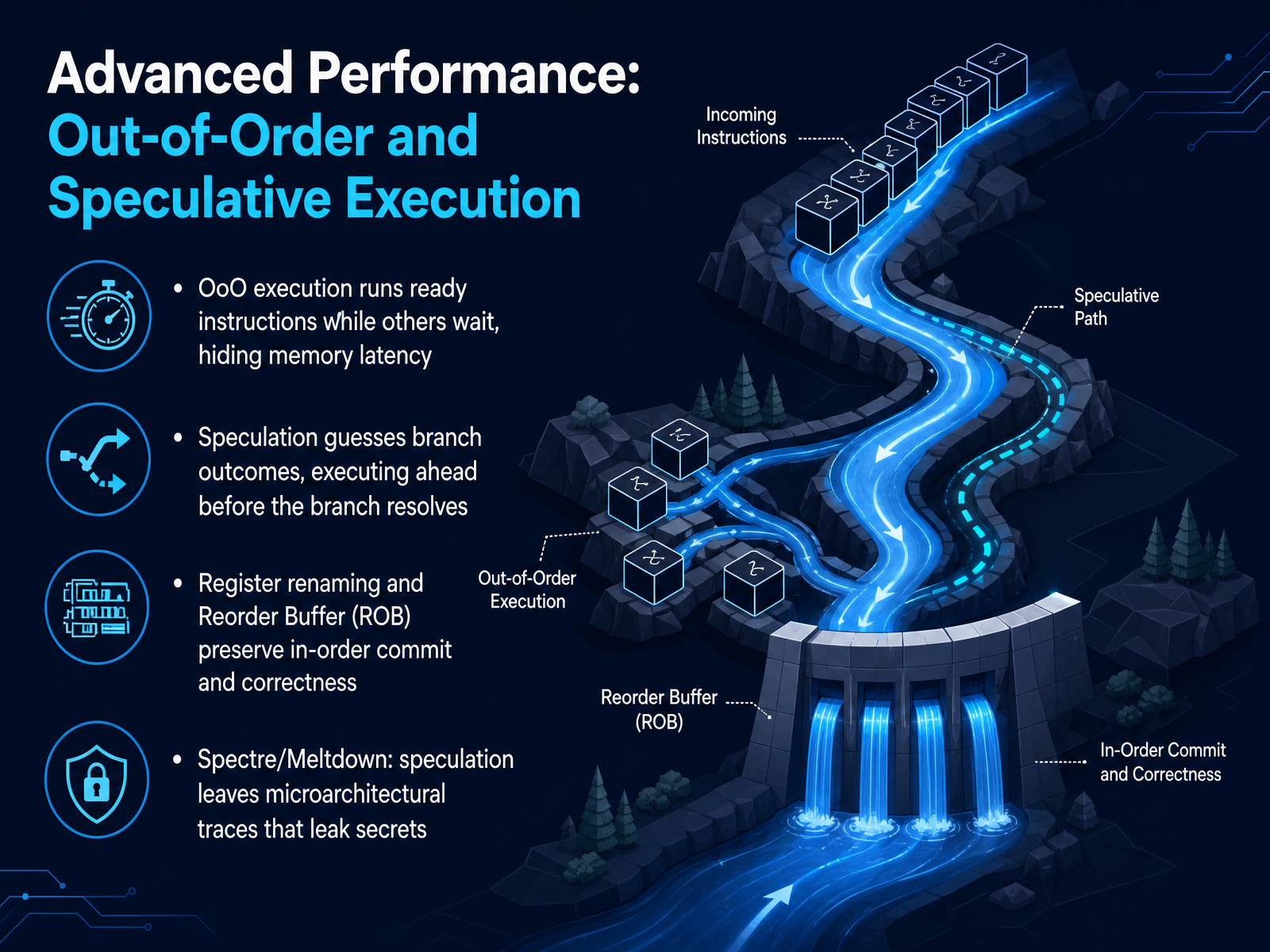
2 min - 11Advanced Performance: Out-of-Order and Speculative ExecutionLet's go deeper into how modern CPUs push performance even further. The title here is Advanced Performance: Out-of-Order and Speculative Execution. Out-of-order execution means the processor can run a ready instruction while an older one is stuck waiting for data from memory. This hides memory latency and keeps the execution units busy. Speculative execution takes this a step further. The CPU guesses the outcome of a branch instruction and starts executing the predicted path before the branch is resolved. To keep all of this safe, the processor uses register renaming and a reorder buffer. These ensure that results are committed in the original program order, maintaining the correct program behavior. However, speculation can leave traces in the microarchitecture, like the cache. This is what the Spectre and Meltdown vulnerabilities exploited, allowing secret data to leak through these side channels. Next, we'll look at how the CPU talks to the rest of the system in Communicating with the Outside World: I/O, Buses, and DMA.
 stackoverflow.comikerexxe.github.iocompilersutra.com+22 min
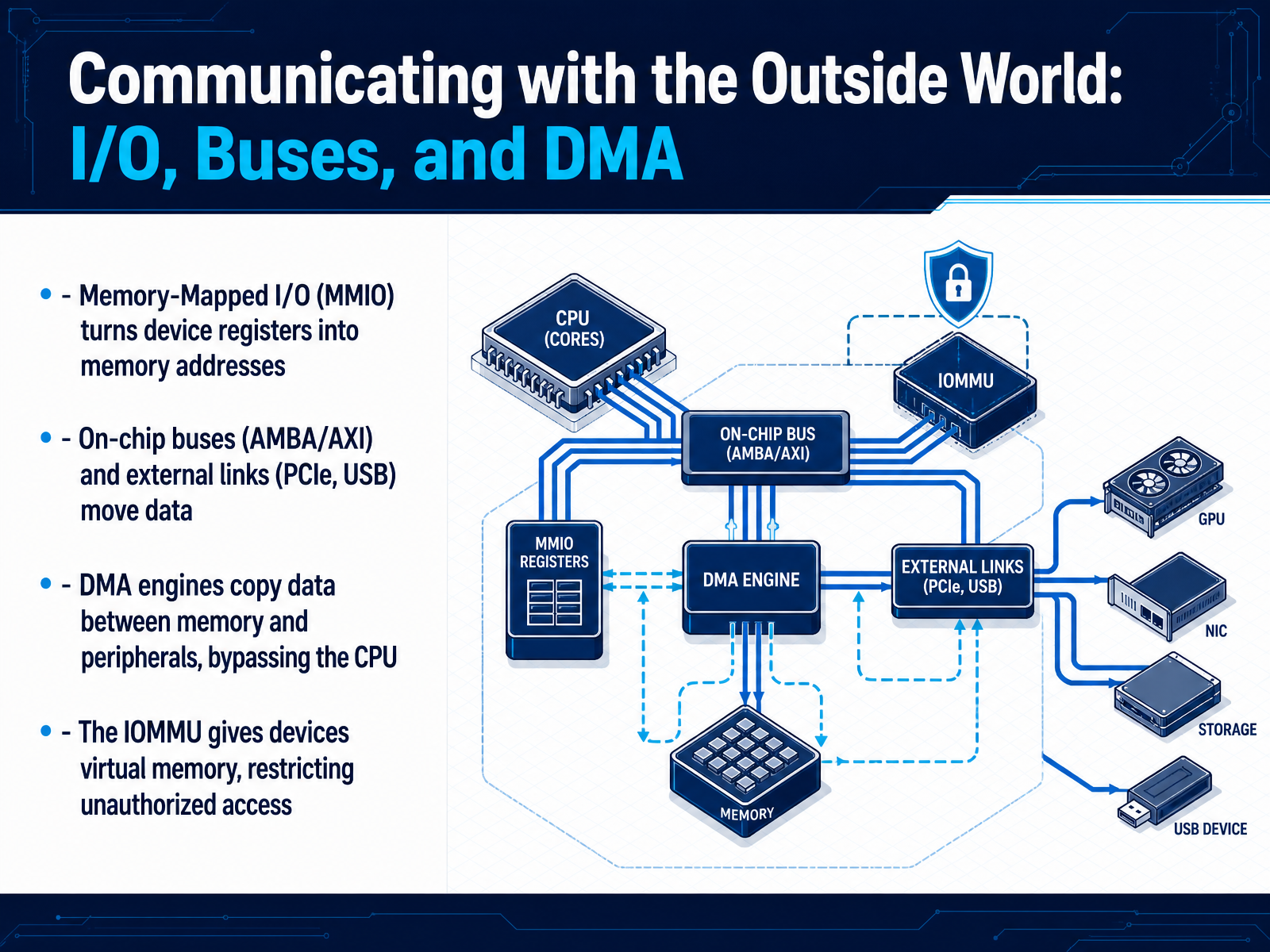
 - 12Communicating with the Outside World: I/O, Buses, and DMANow let's look at how the chip talks to the outside world. When your program reads a file or draws a frame, it needs a way to reach devices like storage, USB, or a display. That communication happens through I/O, buses, and a clever engine called DMA. First, think about how the CPU addresses a device. We use a technique called Memory-Mapped I/O, or MMIO. The device's control registers are simply placed at special memory addresses. To the software, sending a command to a device looks just like writing a value to memory. But how does that data physically travel? Inside the chip, on-chip buses like AMBA and AXI carry the traffic. For external connections, high-speed links like PCIe and USB move data in and out. Now, you might wonder, does the CPU have to manage every single byte? For large transfers, the answer is no. This is where the DMA engine, or Direct Memory Access, steps in. A DMA engine copies data directly between memory and a peripheral, completely bypassing the CPU core. The CPU just sets up the job and then gets back to work. Finally, we have to consider safety. Just like the CPU uses an MMU for virtual memory, devices use an IOMMU. The IOMMU gives each device its own virtual memory map, restricting it to only the memory it is authorized to access. This prevents one device from reading another's data. In short, MMIO and DMA let the system move data efficiently, while the IOMMU keeps those transfers secure. Next, we'll pull all these concepts together as we explore the modern landscape of System-on-Chip Architecture.
 2 min
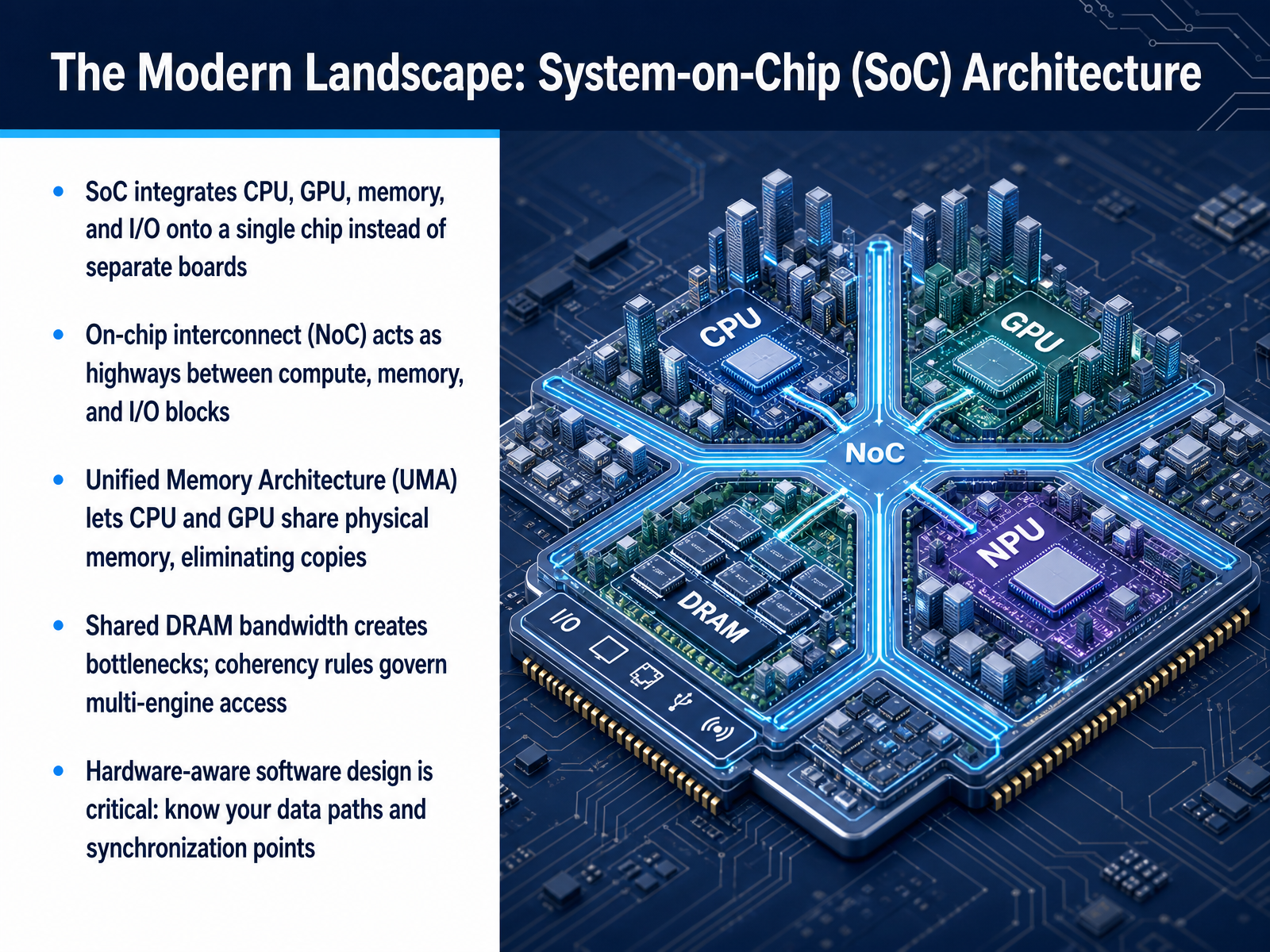
2 min - 13The Modern Landscape: System-on-Chip (SoC) ArchitectureWe've reached the final piece of our architecture puzzle. Let's look at how everything comes together in a modern System-on-Chip, or SoC. An SoC integrates the CPU, GPU, memory controllers, and input-output interfaces onto a single piece of silicon, instead of spreading them across separate boards. This integration is what makes our phones and laptops so compact and power-efficient. The key to making this work is the on-chip interconnect, often called a Network-on-Chip, or NoC. Think of it as a system of highways that lets compute, memory, and I-O blocks talk to each other directly on the die. A major benefit of this design is the Unified Memory Architecture. Here, the CPU and GPU share the same physical DRAM. This eliminates the need to copy data back and forth between separate memory pools, which saves time and energy. However, sharing a single memory channel creates a bottleneck. Since every engine competes for DRAM bandwidth, the system uses coherency rules to govern who can access data and when. This is why hardware-aware software design is critical. As a developer, you need to understand your data paths and synchronization points. Knowing how the hardware shares resources allows you to write code that avoids traffic jams and runs faster. We've covered a lot of ground, from transistors to SoCs. Thank you for sticking with this journey. The hidden logic inside the computer is now a tool you can use. Keep building.
 2 min
2 min
Take the deck with you
Download this course as a file — free, no sign-up needed.
- PDF handoutEvery slide page, ready to print or share.14 pages · 4.2 MBDownload
- Narrated PowerPointThe deck that presents itself — every slide carries the digital human's narration video.14 pages · 14.5 MBDownload
- PowerPoint slidesThe full deck as a .pptx — open it in PowerPoint, Keynote, or Google Slides.14 pages · 4.2 MBDownload
Free to use in your own training — please keep the PersonWise credit page at the end.
Have your own deck? Turn it into a course
Sources consulted
Web sources consulted while building this course.
- Latency Numbers Every Programmer Should Know (2025 Update) — martinkalema.github.io
- Latency Numbers Every Programmer Should Know (2007 vs 2025) | Jincheng Li — jincheng.li
- MartinKalema/latency-numbers — github.com
- Memory Hierarchy Primer — Algorhythm — algo-rhythm.dev
- Michael Tsai - Blog - Latency Numbers Every Programmer Should Know — mjtsai.com
- Architecture, microarchitecture and ISA in microprocessor — cs.stackexchange.com
- Instruction Set Architecture and Microarchitecture — geeksforgeeks.org
- Computer Architecture vs Computer Organization: What Every Compiler Programmer Should Know | CompilerSutra — compilersutra.com
- Architecture and microarchitecture — stackoverflow.com
- Microarchitecture — en.wikipedia.org
- Introduction - CS 61C Course Notes — notes.cs61c.org
- Organization of Computer Systems: Processor & Datapath — cise.ufl.edu
- 250: Datapath and Control — people.duke.edu
- Chapter 4 Processor Part 1: Datapath and Control — dejazzer.com
- A Simple Processor — cs.wellesley.edu
- Out-of-order execution vs. speculative execution — stackoverflow.com
- Tomasulo's algorithm with speculation stages - Iker's Tech Notes — ikerexxe.github.io
- How Modern Processors Execute Code: From Sequential to Speculative Execution | CompilerSutra — compilersutra.com
- How Out-of-Order Execution Works — reorder buffer, register renaming — semicolony.dev
- Perfectionist Programmer — rzmahdi.ir